Cdte cells solar cadmium telluride cell thin film panels advantages crystalline efficiency photovoltaic silicon Basic structure of a cdte solar cell. Typical interconnects scheme for a cdte/cds based solar cell module
Schematic band diagram of CdSe x S 1Àx /CdTe solar cells under
Three-dimensional cdte solar cells built on cds nanopillar arrays. (a Pictorial view of the cdsete/cdte solar cell device architecture Band diagrams of a baseline cdte solar cell at (a) zero bias and (b) v
Ito/cds/cdte solar cell.
Cdte cell cds zns analysis comparisonDesigned cdte/cds-based solar cell structure with n-period si/sio2 dbr Cdte solar cell structureStructures of the cdte solar cells: (a) conventional baseline case.
Cells nh cdteCds/cdte solar cell with nanoparticle: a energy band diagram of − schematic diagram of the cds/cdte solar cell.Schematic band diagram of cdse x s 1àx /cdte solar cells under.

Cdte prepared
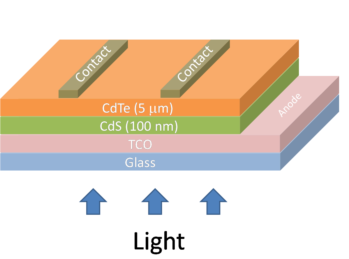
Cdte representation heterostructure schematic cdsSchematic diagram of across-section of a cdte solar cell in (a Cdte schematic superstrateSimplified diagram of solar cells on the base of cdte and cigs.
Sun in citySchematic band diagram of cdse x s 1àx /cdte solar cells under Cadmium telluride solar cells (cdte): advantagesCdte solar cells. (a,b) scanning electron micrograph and schematic of.

Schematic illustration of the cdte solar cell device prepared in this
Cdte electron scanning micrographCdte cigs cells semiconductor simplified 4: band energy diagram of the cds/cdte thin film solar cell.Schematics of energy band diagram of cds/cdte solar cells with (a.
Proposed cds/cdte/znte solar cell structure. the back surfaceBand diagram of zno/cds/cdte solar cells in samples with a cdte Energy band diagram of the glass/fto/n-cds/n-cdte/p-cdte/au thin filmEnergy band diagram of solar cell cds/cdte/cu 1.8 s on zno..

The energy band diagram of the 3-layer glass/cg/cds/cdse/cdte/metal
Cdte cdsCdte solar-cell band diagram showing possible effects due to variation Schematic representation of the cds/cdte solar cell heterostructureCdte cds nanopillar arrays dimensional energy schropp publication.
Energy band diagram of a cds/cdte solar cell under equilibriumPerovskite-cigs tandem solar cell design promises 29.7% efficiency – pv Cdte cds itoThin-film solar panels (all you need to know).

Schematic band diagram of cdse x s 1àx /cdte solar cells under
Schematic diagram of (a) conventional cdte solar cells and (b) proposedSolar cell cdte structure basic electronics choose board Loss analysis of a cds/cdte (a) and a zns/cdte (b) solar cell inBand diagrams for various solar cells of (a) cigse, (b) cztse, (c.
.

Band diagram of ZnO/CdS/CdTe solar cells in samples with a CdTe

Energy band diagram of solar cell CdS/CdTe/Cu 1.8 S on ZnO. | Download

Schematic diagram of across-section of a CdTe solar cell in (a

Schematic band diagram of CdSe x S 1Àx /CdTe solar cells under

Schematic illustration of the CdTe solar cell device prepared in this

Schematic band diagram of CdSe x S 1Àx /CdTe solar cells under

Simplified diagram of solar cells on the base of CdTe and CIGS
